Realization of an array of microcolumns
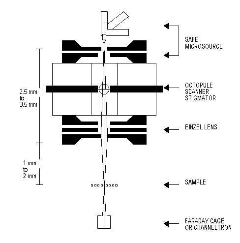
For parallel e-beam lithography miniaturization of the electron optical system is required. Key components of such a system are electrostatic lenses, which typically consist of three electrodes, separated by insulating spacers. Therefore the lenses need to be reduced in size and placed electrically isolated within an array. Up to now only single column systems have been achieved.
In most systems silicon membranes are used as electrodes of the electrostatic lenses and they are supported by silicon as carrier material. With this technique it appears to be difficult to realize an array of electrostatic lenses with electrical isolation between the lenses. We propose the use of borosilicate glass as a carrier material which also acts as insulator and spacer. With this material it is possible to integrate several electrically isolated electrodes, even multipole electrodes, contact pads and interconnections into one surface
The alignment between the electrode holes on different surfaces is another difficulty of lens fabrication. We use the conventional laser-interferometer control of e-beam lithography during exposure of the electrode-holes and alignment marks on the middle electrode-array. These marks enable alignment of the patterning for outer electrodes.
The main process steps for one electrode-array are as follows. The structure of one electrode-array is first etched into a wafer with a 2.5mm thick, highly boron doped epitaxial layer using RIE and a Cr-mask. After stripping the mask a borosilicate glass is connected to the epitaxial layer by anodic bonding. Holes are drilled in the glass by mechanical techniques before bonding. The wafer is finally etched down to the epitaxial layer by a wet chemical etching process.
To produce a lens-array three such electrode-arrays must be bonded together. In our process, the holes in the middle electrode-array and the alignment marks are realized before bonding. The outer two arrays are then bonded. After bonding, the holes in the outer electrodes are also patterned by e-beam lithography and subsequent etching using the alignment marks on the middle electrode-array .
Development of a low profile detector for low energy backscattered electrons
Microcolumns operating at low electron beam energies are under development for application in electron microscopy, spectroscopy and electron beam lithography. Until now only transparent samples and the detection of transmitted electrons have been used to evaluate such systems experimentally. For the intended applicatons backscattered electrons from bulk substrates have to be detected. In developing such a detection system one has to overcome two major problems: small working distance between final lens and sample (~1 mm) and low energy of the electron beam (~1 keV) The first problem requires small detectors like semiconductor diodes. However, the short range of low energy electrons in matter, e.g. less than 50 nm in Si or even less than 20 nm in a Au metal contact layer for 1 keV electrons, prevents the application of conventional semiconductor detectors like surface barrier- or pin-diodes. Therefore we proposed the use of a metal-semiconductor-metal (MSM) structure as a detector for back-scattered electrons in microcolumns.

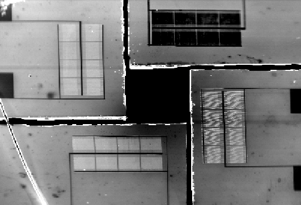
SEM Micrograph of the complete MSM-detector as used for the experiments. The bore in the center is 500 x 500 micrometers.
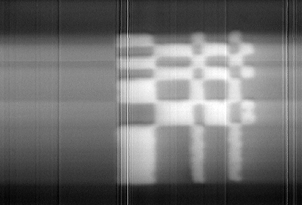
We have developed and tested MSM-detectors for low energy backscattered electrons. The effects of detector symmetry, fingerspacing and detection area on signal to dark current ratio were studied in order to determine an optimized detector geometry. The detector assembly consisting of Ni-GaAs MSM structures with low dark current densities, was mounted in a scanning electron microscope on a special sample holder which allowed us to test the detector under conditions which can be expected in electron beam microcolumn applications. With this experimental setup backscattered electron images of alignment marks of 80 nm thick Au on a Si substrate were obtained. Therefore, it is demonstrated, that MSM-detectors can be used as backscattered electron detectors in microcolumns.[2,3,4]

Micrograph of a 5 micron wide Au marker on Si using the MSM-detector and 1 keV electrons.
References
[1]: T.H.P.Chang, D.P.Kern, L.P.Muray; J.Vac.Sci.Technol. B 6 2743 (1992)
[2]: H.S. Fresser, F.E. Prins, D.P. Kern, Microelectron. Eng. ME-27, 159 (1995)
[3]: H.S. Fresser, F.E. Prins, D.P. Kern, J. Vac. Sci. Technol. B13, 2553 (1995)
[4]: G.D. Meier, H.S. Fresser, F.E. Prins, D.P. Kern, accepted for publication in J. Vac. Sci. Technol. B
return freek.prins@uni-tuebingen.de(freek.prins@uni-tuebingen.de) - Stand 10. August 1996